Physical Cryptanalysis & Hardware Wallet Forensics: Demystifying Chip-Level Extraction
A deep dive into microcontroller architectures, voltage fault injection (glitching), and non-destructive memory recovery standards.
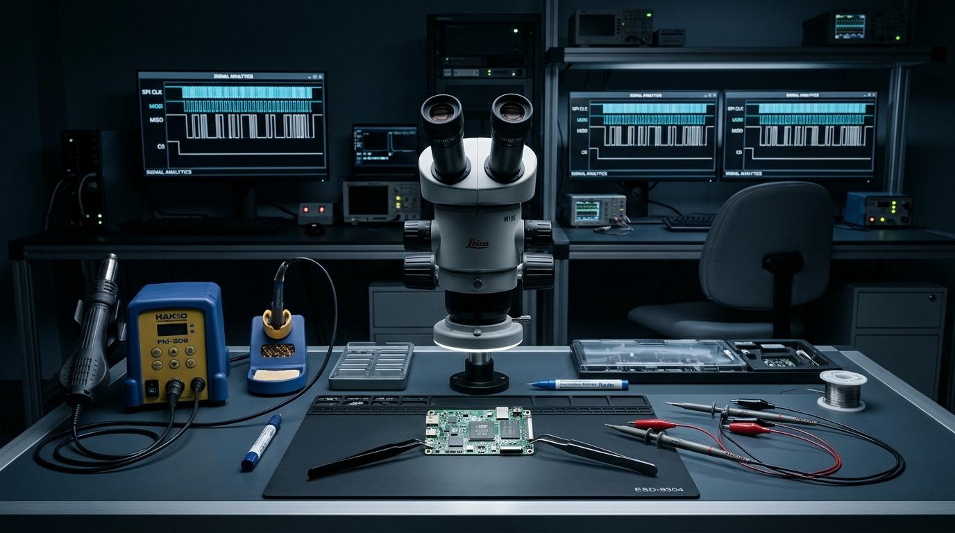
- Silicon Architecture: General-purpose microcontrollers (STM32) vs. Secure Elements (ST33)
- Fault Injection (Glitching): Inducing transient instruction skips via precise voltage drops
- ISO/IEC 27037 Standards: Preserving evidentiary chain-of-custody in cross-border probate estates
The Physical Security Boundary of Cold-Storage Hardware
Cryptocurrency hardware wallets are engineered to keep private keys completely isolated from internet-connected computers. The fundamental security premise is simple: the device signs transactions internally, only transmitting the resulting cryptographic signature back to the host machine.
However, physical hardware devices are susceptible to physical failure modes: forgotten passcodes, lost derivation paths, water immersion, fractured OLED displays, or corrupted NAND flash memory.
In estate probate, cross-border inheritance disputes, and executive device lockups, families and trustees frequently encounter hardware wallets containing substantial generational wealth with zero backup paper seed phrase documentation. Recovering access requires entering the domain of physical cryptanalysis.
General Microcontrollers vs. Certified Secure Elements
To understand how hardware recovery is achieved, one must distinguish between the two primary silicon architectures deployed across the hardware wallet industry.
Legacy and open-source devices (such as early Trezor One and KeepKey models) were constructed around general-purpose commercial microcontrollers, notably the STMicroelectronics STM32 family. These microcontrollers were designed for broad consumer electronics rather than hardened cryptographic defense. While they feature software-level readout protection (RDP), the underlying silicon lacks physical anti-tampering shields or internal clock filters.
In contrast, enterprise-grade devices (such as Ledger Nano series) incorporate dedicated Secure Elements (SEs)—typically Common Criteria EAL5+ or EAL6+ certified chips (such as the ST33 series). Secure Elements utilize active top-layer physical shielding, randomized internal clock generators, dynamic bus encryption, and internal power regulators specifically engineered to defeat physical hardware tampering.
Voltage Fault Injection (VFI) and Instruction Glitching
On devices utilizing general-purpose microcontrollers, one of the most reliable forensic recovery vectors is Voltage Fault Injection, colloquially known as voltage glitching.
When a microcontroller executes its bootloader code, it performs a sequential instruction check to verify whether Readout Protection (RDP Level 1 or 2) is active, or whether a submitted PIN matches the stored cryptographic hash in internal flash memory.
By deploying high-precision pulse generators (such as the ChipWhisperer platform) and monitoring the device's power rail (Vcc) with high-bandwidth oscilloscopes, laboratory cryptanalysts introduce nanosecond-scale voltage drops at the exact clock cycle where the processor evaluates the branch condition: `if (pin_verified == TRUE)`.
The transient voltage starvation causes the CPU pipeline to misexecute the conditional instruction, skipping the branch and allowing the processor to continue execution as though the correct PIN had been provided. This non-destructive bypass enables examiners to read out the encrypted device metadata and reconstruct the 12- or 24-word BIP-39 mnemonic seed phrase.
Cleanroom Micro-Soldering and Trace Reconstruction
In cases of severe physical destruction—such as devices recovered from maritime accidents, vehicle collisions, or structural fires—recovery focuses on physical substrate restoration.
Operating in ISO Class 5 cleanroom conditions under high-magnification stereomicroscopes, forensic engineers carefully desolder the microcontroller, inspect the PCB traces for microscopic hairline fractures, and clean corroded silicon contacts using ultrasonic baths with anhydrous isopropyl alcohol.
If the original circuit board is damaged beyond repair, technicians utilize micro-soldering techniques (using 0.02mm enameled copper wire) to tap directly into the Serial Wire Debug (SWD) and power test points, wiring the chip to an external diagnostic host for non-destructive data imaging.
Evidentiary Chain-of-Custody for Probate and Legal Matters
Technical capability is useless in legal proceedings without rigorous procedural discipline. When VaultGuard is retained by probate attorneys, estate executors, or bankruptcy liquidators, every hardware operation adheres to the international ISO/IEC 27037 standard for digital evidence handling.
Before any diagnostic instrument touches a client device, the physical item is photologged from every angle, serial numbers are cataloged, and initial volatile memory states are documented. All electrical testing parameters (voltage curves, glitch timing offsets, probe contact points) are recorded in an indelible forensic work journal.
Upon successful key derivation, client funds are not moved directly to consultant custody. Instead, recovered key material is transferred under cryptographic dual-control signing protocols to the legal estate administrator's secure custody, ensuring complete judicial compliance and zero tax or conflict complications.
"Hardware wallet recovery is an empirical science requiring cleanroom micro-soldering, fault injection timing, and strict ISO/IEC 27037 chain-of-custody documentation to protect estate assets and probate validity."
Dr. Henrik Lindqvist
CFCE • Hardware Security Lab DirectorDirects complex technical investigations, court-admissible forensic reporting, and jurisdictional asset freezing actions across global institutional digital asset ecosystems.